Sputter Coater for SEM: Important Insights You Must Know
Ever wondered why some SEM scans look like high-definition photos while others are just a blurry mess?
We at Torontech are convinced that a top-tier metal skin is what transforms a mediocre scan into a "wow" result. There is not a hint of fuzzy static anywhere, and the visual clarity is much crisper and more defined.
Key Takeaways
- A highly conductive skin is absolutely non-negotiable: Wrapping your specimen in a microscopically thin metal layer stops frustrating static pile-ups and shields fragile items from intense electron beam heat.
- Your required zoom level dictates your target material: Gold handles everyday visual checks smoothly, Tungsten tackles extreme high-magnification tasks, and Carbon stays completely out of the way for chemical reading.
- The pump system determines the overall capability: Basic metals work perfectly fine in low-vacuum units like our DSR1, but oxygen-hating materials require the heavy-duty pulling action of a high-vacuum system like the DST1-170.
- Actual precision beats simple guessing: Relying on visual estimates for your layer thickness guarantees totally inconsistent results. Utilizing a Quartz Crystal Microbalance guarantees perfectly repeatable finishes every single time you press start.
How Sputter Coating Works
Think of sputtering as a high-speed plating job done inside a heavy-duty, airless steel box.
Our team sucks out the air and pumps in a bit of Argon gas, which gets zapped until it turns into a glowing purple cloud of plasma. These tiny, active gas bits smash into a hunk of metal (your target) so hard they knock off individual atoms. Those atoms then rain down and wrap your sample in a conductive hide that is thinner than a strand of spider silk.
This conductive layer minimizes charging effects during scanning electron microscopy, which significantly improves image clarity and resolution. Every millimeter of this finish is remarkably smooth, and the result is a perfectly wrapped specimen that is ready for the electron beam to do its work.
Advanced methods such as ion beam sputtering can even offer improved coating uniformity at extreme magnifications.
Related article: Spin Coating vs Sputtering: Picking the Best Method
Primary Benefits for SEM Sample Prep
If you try to take a peek at things like bits of plastic, old bone, or tiny bugs without this prep, you are in for a rough time. We see three big reasons why this step is a total necessity:
Eliminating Surface Charging
Take a thick block of synthetic plastic polymer, for instance. When that electron beam hits a material that cannot move electricity, the electrons just pile up on the surface.
It is like a traffic jam that creates ugly white flashes and blurry streaks on your screen. A metal skin gives those electrons a clear path to run away, keeping your view rock-steady.
Enhancing Image Detail and Contrast
Heavy metals are fantastic at spitting back signals. Consider a typical microscopic pollen grain.
By wrapping that dull shape in a layer of gold or platinum, you are essentially turning up the brightness and contrast. It is the difference between an old fuzzy monitor and a crisp high-definition display.
Shielding Thermally Sensitive Samples
Those electron beams are hot. They can melt or shrivel up delicate items, like a fragile slice of biological tissue, in a heartbeat. Sputter coating enhances contrast and preserves these delicate surface details, which is vital for biological specimens that are non-conductive and sensitive to beam damage.
Research and Industrial Use Cases
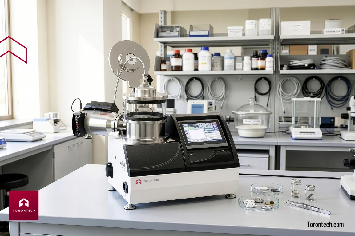
Because non-conductive materials are practically everywhere, we see these machines being used in nearly every field:
- Material Science: Looking at the jagged edges of broken ceramics, like checking the porous surface of a household water filter.
- Life Sciences: Getting crystal-clear views of biological bits, like inspecting the tiny hairs on a fruit fly, without burning them.
- Electronics: Checking out the tiny layers inside microchips to verify structural connections.
- Forensics: Getting the facts from crime scene bits, like pulling chemical data off a piece of clothing fiber or soil.
- Geology & Earth Sciences: Getting the hard facts from rock and dirt, like figuring out the tiny, hidden pores inside a core sample.
- Pharmaceutical Manufacturing: Making sure medical treatments do exactly what they are supposed to do, like examining the slow-release outer shell on a tiny pill.
- Aerospace & Automotive Engineering: Finding out why highly demanding parts fail, like spotting microscopic stress fractures inside a carbon-fiber panel.
- Energy Storage & Batteries: Looking at the inner workings of energy storage units, like inspecting the degrading chemical layers inside a lithium-ion cell.
Choosing the Best Metal for Your Analysis
Choosing your target material is a significant decision. Common target materials include gold, gold-palladium, carbon, and platinum, and they are usually chosen based on imaging needs or whether you need to perform elemental analysis.
| Target Material | Grain Size | Max Zoom | Best Use Case |
|---|---|---|---|
| Gold (Au) | A bit chunky | < 100,000x | Everyday imaging, biological bits |
| Gold/Palladium | Smoother | ~ 100,000x | Better detail, less cracking |
| Platinum (Pt) | Super fine | > 100,000x | High-end nano-work |
| Tungsten (W) | Incredibly tiny | > 200,000x | The highest-resolution scans |
| Carbon (C) | Invisible | EDS/X-ray | Finding out the chemical makeup |
The Quick Breakdown:
- Gold is your reliable old friend. A straightforward unit like our Desk Sputter Coater - DSR1 handles this everyday task smoothly.
- Platinum and Tungsten are for serious high-zoom work. For these ultra-fine jobs, a heavier-duty unit like our High Vacuum, Single Magnetron Target Desk Sputter Coater DST1-170 gets the job done.
- Carbon is the go-to when you need to do chemical analysis, as it does not get in the way of the X-ray signals. A specialized machine like our Desk Carbon Coater - DCR is the standard choice here.
Selecting the Right Hardware Configuration
To get those perfect results, you have to match your metal to the right box.
Low Vacuum vs. High Vacuum
It really comes down to the pump. A simple Low Vacuum setup is great for gold coating everyday samples. But, if you are using fancy metals like Tungsten that hate oxygen, you need a High Vacuum setup with a turbo-pump to suck out every last bit of air.
Check out our full comparison on Low vs. High Vacuum Coaters if you want the technical story: High Vacuum vs Low Vacuum Sputter Coaters Comparison
Comparing Carbon and Metal Deposition
Deciding between carbon and metal often boils down to the specific way you apply the material. Carbon is intensely heated until it turns into a fine vapor. If your daily routine revolves around chemical checks, we suggest a dedicated carbon evaporator, such as our Desk Carbon Coater - DCR.
If your facility handles a mixed bag of daily tasks, you definitely want a two-in-one machine. A piece of hardware like the Desk Sputter & Carbon Coater - DSCR gives you the flexibility to handle both jobs.
For those doing highly intensive research on newly developed materials, we would point you to a heavy-duty multi-target setup, such as our Magnetron Sputtering System ToronSP-400, which can easily manage several heavy metals at the same time.
Related article: A Practical Guide to Pulsed Laser Deposition
Achieving Repeatable, High-Quality Results
We are big believers in getting the settings exactly right. You have to balance how much air is left, how hard you are zapping the metal, and how long you let it run.
Our Professional Advice: Use a Thickness Monitor (QCM).
Honestly, guessing how thick your coating is just does not cut it. We really think a Quartz Crystal Microbalance is a must-have. It tells you exactly how many nanometers you have put down in real-time, ensuring perfectly repeatable sample prep every single time.
Resolving Frequent Coating Obstacles
Even with the best gear, things can get wonky. Challenges such as charging artifacts from residual detritus or uneven coatings can often be resolved by optimizing coating thickness and material choice to maintain topographical fidelity.
Still seeing white flashes? Your coat is likely too thin or did not reach the nooks and crannies. Take a highly textured, bumpy piece of oxidized metal, for example. Those deep valleys easily block the metal spray. We suggest using a rocking or spinning stage to get that metal into every dark corner.
Sample looking melted? You are hitting it with too much heat. Try backing off the energy or using a "pulse" mode where you zap it for a few seconds, let it cool, and zap again.
Image looks like a pile of sand? You have probably put on too much metal or used a chunky metal for a high-zoom shot. Switch to Platinum and use your thickness monitor to keep that layer super thin.
Determining the Best Solution for Your Facility
We are convinced that picking the right prep gear is the only way to truly see what your microscope can do. Whether you need a tiny desk-sized coater for quick gold shots or a heavy-duty high-vacuum system for nano-research, we have a solution that fits.
Ready to stop looking at blurry blobs?
Go take a look at our Sputter Coaters and Vacuum Coating Systems or give our engineering crew a shout to talk about what you are working on. Seriously, what kind of researcher could resist a perfectly crisp, high-resolution result?
References:
- Chissoe, W. (1996). Combining Sputter Coating with OTOTO Treatment to Eliminate Charging Artifacts in Pollen Preparations. 76, 83-85.
- Clay, C., & Peace, G. (1981). Ion beam sputtering: an improved method of metal coating SEM samples and shadowing CTEM samples. Journal of Microscopy, 123.
- Fischer, E., Hansen, B., Nair, V., Hoyt, F., Schwartz, C., & Dorward, D. (2024). Scanning Electron Microscopy. Current protocols, 4, e1034 - e1034.
- Heu, R., Shahbazmohamadi, S., Yorston, J., & Capeder, P. (2019). Target Material Selection for Sputter Coating of SEM Samples. Microscopy Today, 27, 32 - 36.
- Mentor, S., Cummings, F., & Fisher, D. (2021). Preparation of biological monolayers for producing high-resolution scanning electron micrographs. PLoS ONE, 17.