Carbon Coater vs Sputter Coater: Full Lab Comparison
Are charging flares, thermal distortion, and blurry resolution compromising your electron microscopy data?
Deciding whether to install two separate dedicated instruments or invest in a consolidated benchtop dual sputter and carbon coater comes down to bench space, budget, and your specific analytical requirements. Here is our direct technical comparison to help you configure the ideal platform for your facility.
Deposition System Comparison Matrix
| Evaluation Criteria | Standalone Sputter Coater | Standalone Carbon Coater | Dual Sputter and Carbon Coater / Combined SEM Coater |
|---|---|---|---|
| Primary Mechanism | Magnetron plasma sputtering | Thermal evaporation of carbon fiber or rods | Integrated magnetron sputtering and carbon evaporation |
| Typical Target Sources | Au, Pt, Pd, Au/Pd alloys (plus Ir, Cr, W on high-vacuum models) | High-purity carbon fiber, carbon yarn, graphite rods | Noble metals and carbon fiber (rotary-pumped units); oxidizing targets such as Cr, W, and Ir require turbo-pumped models |
| Primary Analytical Focus | Topographic SEM and FE-SEM secondary electron imaging | Quantitative EDS, WDS, EBSD, and TEM support grids | Versatile: imaging, elemental spectroscopy, and research films |
| Cross-Contamination Risk | Not applicable (Dedicated metal chamber) | Not applicable (Dedicated carbon chamber) | Managed via source isolation, shutters, and dedicated inserts |
| Footprint and Capital Expense | Single benchtop footprint; dedicated instrument CapEx | Single benchtop footprint; dedicated instrument CapEx | Consolidates two capabilities into a single benchtop footprint; cost-effective |
| Best Suited For | High-volume routine imaging facilities | Dedicated microprobe, geochemical, or TEM laboratories | Multi-user core facilities, universities, and mixed-use labs |
Deposition Physics: Carbon Coater vs Sputter Coater
From an engineering perspective, we consider the choice between metal sputtering and carbon evaporation to be one of the most frequently oversimplified trade-offs in electron microscopy. When non-conductive specimens encounter an incident electron beam in an SEM, accumulated negative charges cannot dissipate.
The resulting charge buildup creates severe visual artifacts across your display: blinding flares, beam deflection, distorted sample geometry, and localized thermal damage. Applying a thin conductive layer resolves these issues, but the proper deposition method depends entirely on your downstream analytical goals.
Metal Sputtering: Topography and Secondary Electron Yield
Sputtering operates through direct physical momentum transfer: accelerated argon ions strike a solid metal target, dislodging fine metal atoms that settle across your specimen in an even, continuous blanket. Heavy noble metals such as gold (Au), platinum (Pt), palladium (Pd), and mixed gold-palladium (Au/Pd) alloys release a high volume of secondary electrons. This yields exceptional edge definition, rich contrast, and micrographs with distinct topographic depth.
In a comparative evaluation of biological monolayers, mouse brain endothelial cells coated with Au:Pd revealed fine intercellular nanotubes, crisp cellular margins, and small surface features with outstanding structural clarity. In contrast, parallel specimens prepared with carbon produced an indistinct, low-contrast field where fine membrane details were difficult to resolve from the background.
However, metal deposition involves distinct analytical compromises. Heavy metal coatings can agglomerate into granular island formations during high-magnification field-emission inspection. In our assessment, while gold remains an accessible baseline, investing in platinum or palladium targets offers superior value for high-resolution work because it avoids coarse grain clustering.
Additionally, heavy metals produce prominent characteristic X-ray lines (such as gold M-family lines between 2.12 keV and 2.20 keV) that directly overlap with light elements like sulfur and phosphorus, as well as transition metal lines like zirconium and molybdenum L-series, complicating elemental identification.
Carbon Evaporation: Low-Z Microanalysis and Spectroscopy
Carbon evaporation takes an alternative approach. Passing controlled electrical current through carbon fiber threads or high-purity graphite rods inside a vacuum chamber sublimates the carbon into vapor, condensing across the samples below. Because carbon has a low atomic number (Z = 6), a fine carbon layer provides an electrical discharge pathway to ground while remaining virtually transparent to outgoing characteristic X-rays.
In our view, attempting quantitative EDS or light-element identification on heavy-metal sputtered samples introduces severe peak overlap risks that clean carbon evaporation avoids. This spectral neutrality makes carbon deposition the recognized standard for quantitative Energy Dispersive X-ray Spectroscopy (EDS), Wavelength Dispersive X-ray Spectroscopy (WDS), and Electron Probe Microanalysis (EPMA).
When applied as an ultra-thin layer around 2.5 to 5 nm (or left uncoated under low-vacuum SEM conditions), carbon also supports crystallographic orientation mapping via Electron Backscatter Diffraction (EBSD), as thicker carbon layers noticeably weaken Kikuchi diffraction patterns.
Typical Industry Coating Thickness Benchmarks
In general microscopy practice, target film thicknesses vary by analytical goal:
- Routine SEM Topography: 5 to 20 nm of Au or Au/Pd
- High-Magnification FE-SEM: 1 to 5 nm of fine-grain Pt or Ir
- Standard EDS/WDS Microanalysis: 10 to 20 nm of carbon
- EBSD Orientation Mapping: Roughly 2.5 to 5 nm of carbon
Because hitting single-nanometer tolerances reliably is difficult by visual estimation alone, thin-film applications below 5 nm generally require a high-vacuum coater paired with calibrated Quartz Crystal Microbalance (QCM) monitoring rather than a basic timed rotary unit.
Core Takeaway: When the priority is morphological imaging and secondary electron contrast, a sputter coater is the preferred tool. When conducting quantitative elemental spectroscopy or routine electron backscatter diffraction on non-conductive specimens, a carbon coater is generally the recommended choice.
Combined SEM Coater Architecture and Vacuum Regimes
Early microscopy literature demonstrated that depositing carbon and metal sequentially within a single chamber saved significant preparation time while protecting sensitive surfaces from atmospheric exposure. Modern combined SEM coater hardware expands on this practical concept through modular engineering.
Modular Interchangeable Source Heads
In our assessment, modular quick-swap heads represent an intelligent operational solution for facilities with limited benchtop space.
Instead of purchasing two independent consoles, operators can switch between a magnetron sputter head (driven by direct current for noble metals or optional radio-frequency supplies for insulating targets) and a pulsed carbon evaporation head (utilizing carbon fiber threads or graphite rods) on a shared vacuum chassis. This approach minimizes initial capital expenditure and consolidates routine vacuum pump servicing to a single mechanical or turbomolecular pumping station.
Vacuum Regimes and Pumping Configurations
We always encourage facility directors to evaluate their vacuum architecture just as carefully as their target selections, because vacuum depth governs film purity and microstructure:
- Low-to-Medium Vacuum Regimes: Operating at fore-vacuum pressures around 7 x 10^-3 mbar using a two-stage rotary vane pump, these systems serve as reliable workhorses for routine tungsten-filament SEM imaging and general carbon thread evaporation.
- High-Vacuum Regimes: Utilizing an integrated turbomolecular pump to achieve base pressures of 10^-5 Torr to 10^-7 mbar. This high-vacuum regime extracts residual hydrocarbons and water vapor, which we consider necessary for sputtering reactive or oxidizing metals (such as chromium or tungsten), depositing ultra-fine grain films for Field Emission SEM (FE-SEM), and ensuring high-purity carbon films.
Surface Modification and Glow Discharge
To extend functional capability, these deposition chambers can be configured to run glow-discharge surface treatments on carbon support films. In our view, an integrated glow-discharge feature provides substantial value for transmission electron microscopy (TEM) sample preparation, converting hydrophobic carbon grids into hydrophilic surfaces so biological suspensions and negative stains spread uniformly without droplet bead-up.
Cross-Contamination Control in Dual Systems
A frequent concern raised regarding combined deposition systems is the potential for cross-contamination, specifically whether residual metal atoms could deposit onto samples prepared for sensitive EDS microanalysis. In our technical assessment, this risk is thoroughly managed when systems incorporate proper mechanical safeguards:
- Source Isolation and Dedicated Heads: Physically isolating the sputtering target from the carbon evaporation source prevents stray material transfer during active deposition cycles.
- Automated Mechanical Shutters: Motorized metal shutters shield specimens during plasma stabilization and initial source outgassing, opening only when the vapor stream is stable and closing instantly once the target thickness is reached. We consider automated physical shutters far superior to manual levers because automated timing eliminates operator variability during initial source outgassing.
- Pulsed Evaporation Modes: Delivering short-duration, high-current electrical pulses through carbon fibers restricts radiant thermal load and significantly reduces loose particulate carbon debris compared to continuous flash techniques, helping maintain cleaner internal surfaces.
Dual Coaters vs. Dual Magnetron Co-Sputtering
Vacuum literature uses the term "dual" in two distinct ways that buyers should separate before selecting equipment. In SEM sample preparation, a "dual coater" refers to a benchtop system integrating metal sputtering and thermal carbon evaporation. In materials science and physical vapor deposition (PVD), "dual sputtering" describes firing two or more magnetron cathodes simultaneously (such as a metallic target alongside a graphite target) in academic research to synthesize hard, wear-resistant metal-carbon nanocomposite films.
For laboratories moving beyond routine microscopy preparation into functional thin-film research, Torontech offers dedicated multi-cathode platforms rather than standard dual prep coaters. Specifically, the DST3-A configuration within our DST3-A/S series features three angled 2-inch water-cooled magnetron cathodes with DC and optional RF supplies built for alloy deposition and co-sputtering workflows, while the DST2-TG pairs double 2-inch magnetron targets with thermal evaporation for multi-material research.
North American Laboratory Application Profiles
From our perspective as an equipment manufacturer, laboratory instrumentation requirements across the United States and Canada generally fall into three distinct operational categories:
Academic Shared-Facility Environments
University core imaging facilities (such as multi-user centers funded by NSF grants in the United States or NSERC and CFI programs in Canada) routinely support diverse departmental users. A single system may prepare biological monolayers in the morning and metallurgical samples in the afternoon. In our view, a multi-functional dual system represents the most practical investment for these facilities, meeting both high-resolution imaging and elemental microanalysis needs on a single benchtop while conserving capital funds.
Geochemical and Natural Resource Operations
Commercial assay and testing facilities (such as mineral exploration laboratories across mining districts in Ontario and Quebec, or geological testing hubs in Nevada and Colorado) operate under distinct production requirements.
High-throughput automated mineralogy, QEMSCAN, and electron microprobe analysis require continuous carbon coating of polished thin sections and core mounts. In our assessment, deploying a dedicated, high-vacuum carbon coater is the most reliable strategy for these facilities, completely eliminating the risk of trace heavy-metal contamination during automated mineral phase mapping.
Microelectronics and Semiconductor Inspection
In commercial semiconductor corridors and cleanroom environments, microscopy facilities inspect wafer fragments, packaged devices, and patterned substrates. In our view, spacious vacuum chambers equipped with multi-inch target cathodes, motorized substrate stage rotation, and adjustable working distances are operational necessities here, ensuring uniform, defect-free deposition across wide semiconductor substrates without edge-shadow effects.
Torontech Equipment Portfolio
Torontech provides an extensive portfolio of cost-effective desk sputter coaters and vacuum coating systems built to meet demanding analytical standards:
Dedicated Sputter Systems
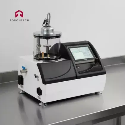
For routine electron microscopy imaging, we view the compact Desk Sputter Coater - DSR1 as a dependable rotary-pumped platform achieving an ultimate base vacuum below 40 mTorr to deposit uniform films of gold (Au), palladium (Pd), platinum (Pt), and gold/palladium (Au/Pd).
If your facility requires dedicated high-vacuum conditions for high-resolution FE-SEM preparation, the single-target DST1-170 is an ideal fit, supporting fine-grain deposition of noble metals (Au, Pt/Pd, Ag) as well as iridium (Ir), chromium (Cr), and tungsten (W). When handling larger substrates, the DST1-300 provides an expanded chamber built for semiconductor wafers, while the DST3-A/S integrates turbomolecular pumping and three magnetron targets for complex multi-layer thin-film deposition.
Dedicated Carbon Systems
For facilities focused strictly on elemental microanalysis, the compact Desk Carbon Coater - DCR provides a dependable carbon fiber deposition platform for standard SEM preparation. For laboratories operating high-resolution FE-SEM, EDS/WDS, TEM, or EBSD instruments, we recommend the Turbo Pumped Desk Carbon Coater- DCT, which maintains a clean high vacuum for debris-free carbon deposition. For high-volume geological sample batches, the DCT-300 incorporates the same turbomolecular pumping system into a spacious vacuum chamber.
Combined and Multi-Target Platforms
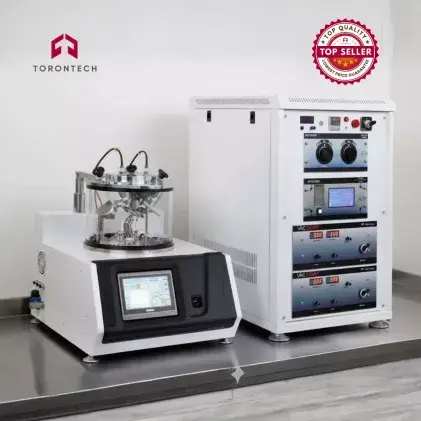
If your laboratory requires maximum versatility on a single benchtop, our combined systems provide an all-in-one solution. The rotary-pumped Desk Sputter & Carbon Coater - DSCR integrates noble metal sputtering and carbon fiber evaporation below 50 mTorr in a space-saving chassis, while the DSCR-300 accommodates higher batch throughput with a large chamber and 3 or 4-inch water-cooled magnetron cathodes.
For facilities requiring a high-vacuum operating environment for noble metal sputtering alongside pulsed carbon fiber evaporation, the turbomolecular-pumped High Vacuum Desk Sputter & Carbon Coater - DSCT provides an optimal dual-capability platform.
For specialized thin-film research, our multi-method platforms handle advanced deposition requirements. The DSCT-T integrates high-vacuum sputtering with carbon and thermal evaporation sources built for SEM sample preparation. Thin-film research laboratories can utilize the DST2-TG (pairing double magnetron targets with thermal evaporation) or the DST3-TA/S (DST3-T) (combining three magnetron targets with thermal evaporation).
Furthermore, plasma cleaning functionality comes built into desk models such as the DSR1, DST1-170, DST1-300, DCR, DCT, DSCR, and DSCR-300 to remove organic surface contaminants prior to deposition, and is available as an optional feature on the DST2-TG and DST3-A/S.
Find Your Ideal Torontech Dual Coater Solution
Whether your facility requires a dedicated high-resolution sputter coater, an analytical carbon coater, or a versatile dual sputter and carbon coater, Torontech provides cost-effective, high-precision equipment matched to your laboratory standards.
Contact our engineering team today to review your specific microscopy applications, examine technical specifications, or receive a customized equipment quotation for your laboratory.
References (Click to expand)
- Benada, O., & Pokorný, V. (1990). Modification of the Polaron sputter-coater unit for glow-discharge activation of carbon support films. Journal of Electron Microscopy Technique, 16(3), 235-239.
- Cummings, F., & Fisher, D. (2021). Comparative analysis of coating modalities for producing high resolution textured micrographs v2. protocols.io.
- Fischer, E. R., Hansen, B. T., Nair, V., Hoyt, F. H., Schwartz, C. L., & Dorward, D. W. (2024). Scanning electron microscopy. Current Protocols, 4(4), e1034.
- Heu, R., Shahbazmohamadi, S., Yorston, J., & Capeder, P. (2019). Target material selection for sputter coating of SEM samples. Microscopy Today, 27(4), 32-36.
- Ltd., K. I. (2014). Sample preparation for translucent and scanning electron microscopy: New Leica Microsystems coaters. Science and Innovation, 10(2), 50-54.
- Mentor, S., Cummings, F., & Fisher, D. (2021). Preparation of biological monolayers for producing high-resolution scanning electron micrographs. PLoS ONE, 16(6), e0266943.
- Namork, E. (1985). Preparation of carbon films from evaporated fibers and rods at fore-vacuum pressure. Journal of Electron Microscopy Technique, 2(1), 45-51.
- Nedfors, N., Tengstrand, O., Lewin, E., Furlan, A., Eklund, P., Hultman, L., & Jansson, U. (2011). Structural, mechanical and electrical-contact properties of nanocrystalline-NbC/amorphous-C coatings deposited by magnetron sputtering. Surface & Coatings Technology, 206(2-3), 354-359.
- Onoprienko, A., Ivashchenko, V., Scrynskyy, P., Kozak, A., Ťapajna, M., & Orovčík, Ľ. (2021). Structural and mechanical properties of Ti-B-C coatings prepared by dual magnetron sputtering. Thin Solid Films, 730, 138723.
- Pretorius, E. (2011). Traditional coating techniques in scanning electron microscopy compared to uncoated charge compensator technology: Looking at human blood fibrin networks with the ZEISS ULTRA Plus FEG-SEM. Microscopy Research and Technique, 74(12), 1171-1178.