
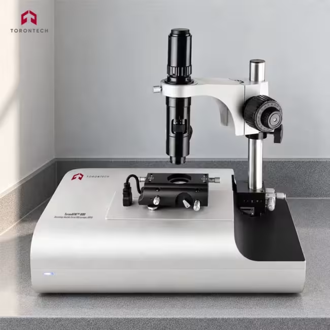
Benchtop Atomic Force Microscope (AFM) - ToronAFM™ 600
ToronAFM™ 600 benchtop atomic force microscope delivers nanoscale surface imaging from a standard laboratory bench. The system resolves 1 nm of lateral detail and 0.1 nm of vertical detail, producing quantitative topography without a dedicated instrument room. Materials scientists, semiconductor engineers, polymer chemists, and life science teams use it to map roughness, grain structure, and thin film uniformity. Control electronics, a 21-inch all-in-one computer, and imaging software ship as one plug-and-play package.
Three standard imaging modes cover most sample types: contact, non-contact, and tapping. Contact mode suits hard, flat surfaces, while tapping mode protects soft polymers and biological specimens that a dragging tip would damage. Optional functional kits add magnetic, electrical, and mechanical characterization, so one bench instrument can serve several research groups. The motorized stage travels 15 mm in each axis with 40 nm steps, letting operators reach any point on a 20 mm sample under software control.
Setup time stays short because the ToronAFM™ 600 connects to any Windows computer over a single LAN cable. A top-view optical microscope with 8-megapixel color imaging and 60X to 600X zoom lets the operator pick a scan site before the probe engages. Automatic fast approach then brings the cantilever to the surface without manual adjustment or risk of tip damage. Laboratories gain usable images in minutes and keep the bench space they would otherwise surrender to a floor-standing platform.
Benchtop Atomic Force Microscope (AFM) - ToronAFM™ 600 Applications
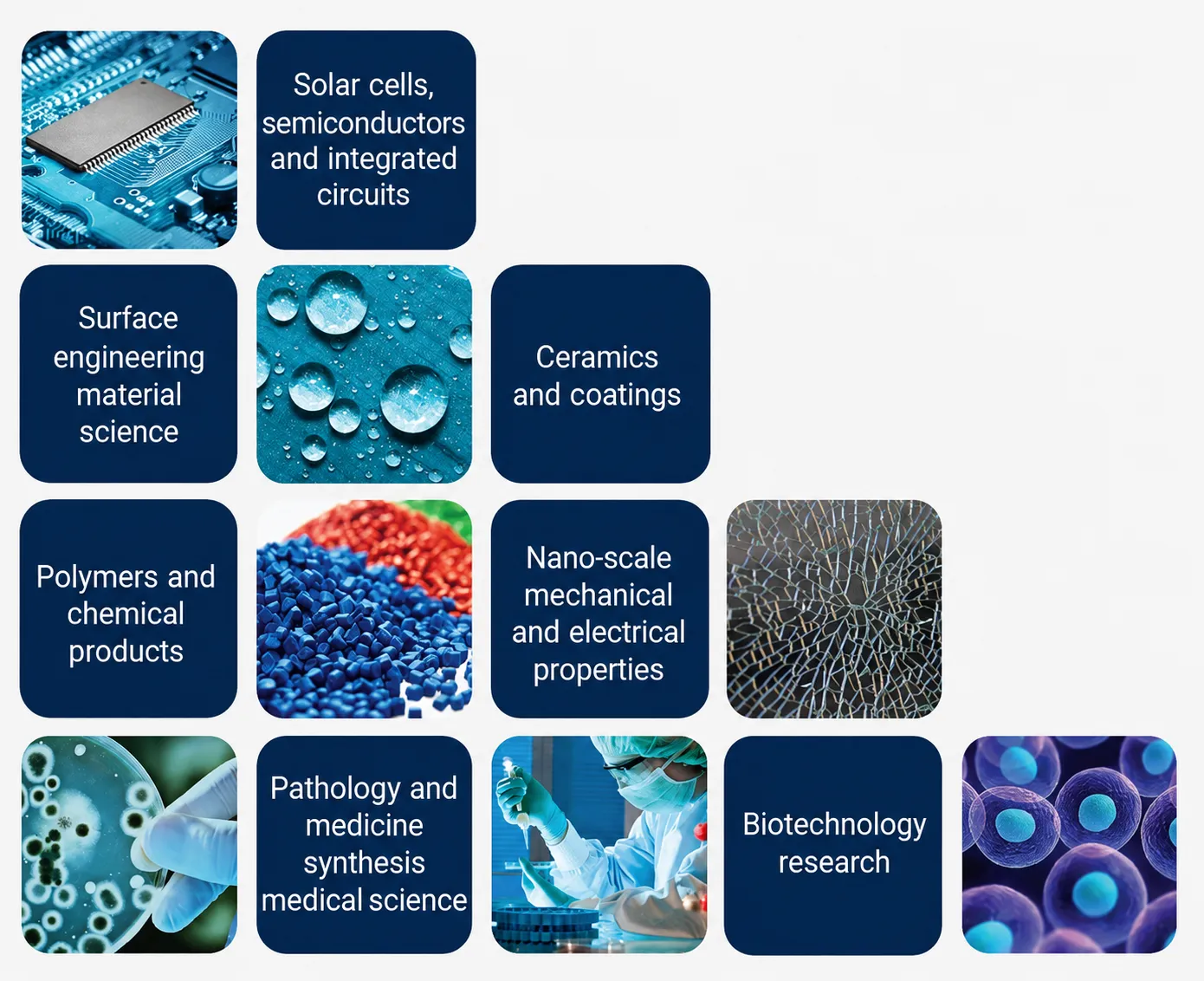
The ToronAFM™ 600 supports surface characterization wherever features below the optical diffraction limit determine performance. Its compact footprint and short setup cycle suit shared laboratories that run mixed sample types across several projects.
- Semiconductors and Integrated Circuits: measures step heights, line edge roughness, and wafer surface quality during process development and failure analysis
- Solar Cells and Photovoltaics: maps texture, grain boundaries, and local conductivity across absorber layers and transparent electrodes
- Surface Engineering and Materials Science: quantifies roughness, wear tracks, and grain morphology on treated and untreated metal surfaces
- Ceramics and Coatings: verifies coating uniformity, porosity, and adhesion-related surface texture on thin and thick films
- Polymers and Chemical Products: resolves phase separation, crystallinity, and blend morphology using phase imaging on soft samples
- Nanoscale Mechanical and Electrical Characterization: acquires force curves, stiffness maps, and local current data with optional functional kits
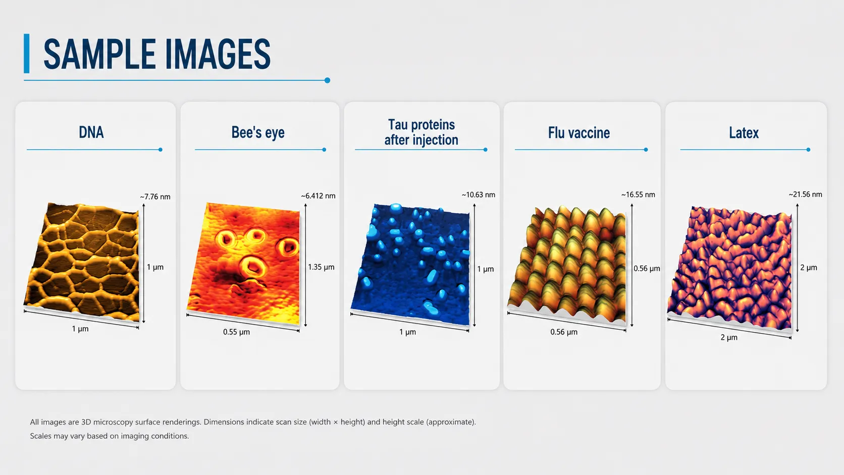
- Biotechnology Research: images DNA strands, proteins, cell membranes, and viral particles in air with minimal sample preparation
- Pathology and Medical Science: examines tissue structures, protein aggregates, and drug delivery carriers at nanometer scale
- Pharmaceutical and Vaccine Development: characterizes particle size, surface morphology, and aggregation behavior in formulations
- Academic Teaching and Research Laboratories: gives students hands-on scanning probe experience on an instrument small enough for a shared teaching lab
Benchtop Atomic Force Microscope (AFM) - ToronAFM™ 600 Key Features
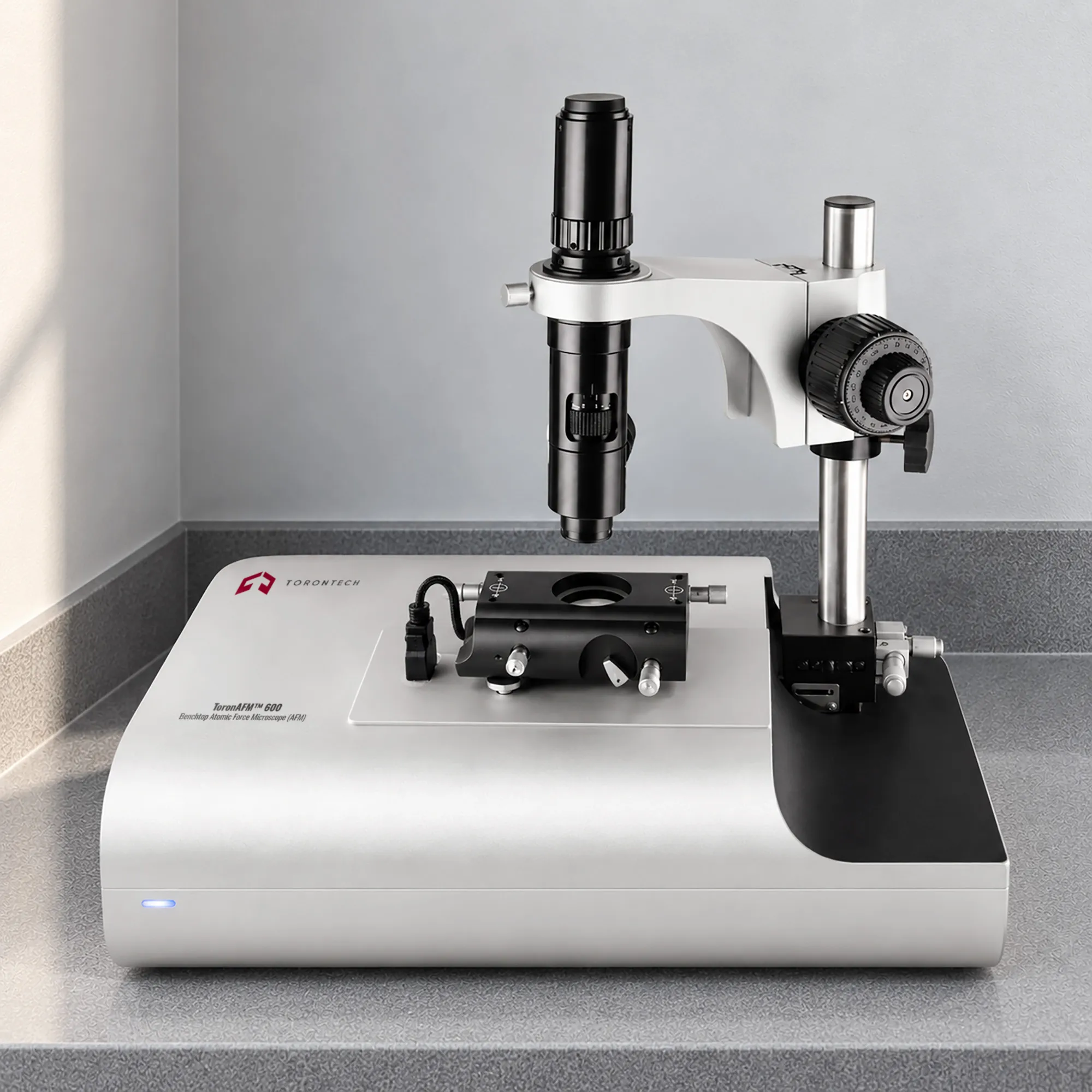
The ToronAFM™ 600 combines a redesigned scan head, 24-bit control electronics, and a single-cable interface to shorten the path between sample loading and finished image.
- 1 nm XY and 0.1 nm Z Resolution: resolves surface features well below the optical limit for quantitative roughness and step height work
- Automatic Fast Approach: engages the cantilever to the sample surface from any starting distance without operator input, cutting setup time and protecting the tip
- Simplified Tip Fixation: a spring lever holder and vacuum pen let operators seat a probe quickly with low risk of breakage
- Chip Alignment Template: positions the cantilever chip repeatably so laser alignment carries over between probe changes
- Reduced Head Weight: lighter scan head makes handling and micrometer adjustment easier during routine operation
- Adjustable Laser Optical Path: operators tune the optical alignment by shifting the beam path instead of repositioning the detector
- 8-Megapixel Top-View Optical Microscope: 60X to 600X color zoom with integrated dimmable lighting shows the scan site before the probe engages
- Single LAN Cable Connection: one network cable carries all data and control traffic at 100 MB/sec, removing the usual cable bundle from the bench
- Remote Network Operation: any workstation on the network can run the instrument, and a technical specialist can join the same session for troubleshooting
- 24-Bit Data Conversion: four ADC and four DAC channels at 24-bit depth preserve fine signal detail across the full scan range
- Zynq Signal Processing Platform: handles feedback and acquisition in real time for stable imaging at speed
- Integrated Signal Oscilloscope: displays every system signal live so operators can diagnose scan quality while the image forms
- Zoom Rescan of Captured Images: select a region on a finished scan and acquire it again at higher pixel density without reloading the sample
- Automatic Image Gallery Saving: captured scans store themselves in an organized library, reducing the chance of lost data
- Independent Analysis Software: a separate processing package handles flattening, measurement, and presentation, and exports image data in several formats
- Sample Bias Control: applies -10 V to +10 V across the sample for electrical characterization work
- Three Standard Modes: contact, non-contact, and tapping ship with every unit, covering hard, soft, and delicate samples
- Modular Functional Kits: add magnetic, electrical, mechanical, and lithography techniques to the same platform as research needs grow
- Compact 300 x 400 x 300 mm Footprint: fits on a shared bench at 20 kg, so no dedicated instrument room is needed
- Windows Compatibility Across Hardware: runs on desktops, laptops, and all-in-one machines, and ships with a dedicated 21-inch all-in-one computer
Theory and Method
Atomic force microscopy maps a surface by measuring the force between a sharp tip and the sample rather than by focusing light or electrons. The tip sits at the free end of a flexible cantilever only a few micrometers thick. As the tip nears the surface, van der Waals attraction, electrostatic forces, and short-range repulsion bend the cantilever by a fraction of a nanometer. That deflection carries the topographic signal.
A 670 nm laser diode reflects off the back of the cantilever onto a four-segment photodiode. Bending shifts the reflected spot across the detector segments, and the difference in segment currents scales with deflection. The controller compares this signal against a setpoint and drives the Z piezoelectric scanner up or down to hold the force constant. Recording the Z voltage at every XY position builds the height map. Optical lever amplification turns sub-nanometer bending into a measurable signal.
Contact mode holds the tip against the surface and tracks deflection directly, which gives fast scans on rigid samples. Tapping and non-contact modes drive the cantilever near resonance with a dithering mechanism and track changes in oscillation amplitude or phase. Because the tip touches only briefly or not at all, soft biological and polymer samples survive imaging intact. Lift-mode techniques such as MFM and KPFM run a second pass above the recorded topography, separating magnetic or electrostatic signals from surface shape.
Benchtop Atomic Force Microscope (AFM) - ToronAFM™ 600 Technical Specifications
| Parameter | Specification |
|---|---|
| Scanner | |
| XY Scan Range | 20 µm to 70 µm maximum |
| XY Resolution | 1 nm |
| Z Movement Range | 4 µm maximum |
| Z Resolution | 0.1 nm |
| Stage | |
| XY Stage Type | Motorized, software-controlled |
| XY Travel Range | 15 mm |
| XY Movement Step | 40 nm |
| Z Travel Range | 15 mm |
| Z Movement Step | 40 nm |
| Cantilever Engage | Automatic (Auto Fast Approach) |
| Sample Mount | |
| Maximum Sample Diameter | 20 mm |
| Maximum Sample Thickness | 10 mm |
| Sample Holder | Light magnetic sample holder included |
| Sample Bias Voltage Range | -10 V to +10 V |
| Scan Head | |
| Adjustment | High-precision micrometer |
| Laser Wavelength | 670 nm |
| Maximum Laser Diode Power | 5 mW |
| Photodetector | High-grade quadruple photodiode |
| Excitation | Dithering mechanism |
| Optical Path | Optimized design |
| Tip Holder | Spring lever mechanism |
| Top-View Optical Microscope | |
| Camera Resolution | 8 megapixel, color |
| Optical Zoom | 60X to 600X |
| Illumination | Integrated, with dimmer |
| Electronics | |
| Control Box | Plug and play |
| ADC Channels | 4 channel, 24-bit |
| DAC Channels | 4 channel, 24-bit |
| Signal Processing | 40 MHz Zynq processor |
| Data Transfer | 100 MB/sec via LAN |
| Software | |
| Data Acquisition | Real-time, 100 MB/sec, Microsoft Windows compatible |
| Optical View | Integrated windows for sample and cantilever vision |
| Signal Monitoring | High-rate oscilloscope across all system signals |
| Image Storage | Automatic saving to software gallery |
| Zoom Scanning | Rescan of a selected area on captured images |
| Approach | Automatic fast approach of cantilever to sample surface |
| Image Processing | Independent software for processing, analysis, and presentation |
| Data Export | Multiple image data export formats |
| Operating System | Compatible with all Microsoft Windows versions |
| Imaging Modes (Standard) | Contact, Non-Contact, Tapping |
| Dedicated All-in-One Computer | |
| Display | 21 in, 1920 x 1080 |
| Processor | Latest generation |
| Memory | 8 GB RAM |
| AFM Unit | |
| Installation | Plug and play |
| Dimensions (W x D x H) | 300 x 400 x 300 mm |
| Net Weight | 20 kg |
Included Accessories
| Item | Description |
|---|---|
| Sample Mounting Kit | Hardware for securing samples to the stage |
| Sample Substrate | Substrate for sample preparation and mounting |
| Cantilevers | Assorted probe types for the standard imaging modes |
| Tweezers and Magnet Box | Handling tools and storage for probes and magnetic holders |
Optional Upgrades
| Item | Description |
|---|---|
| Extended XY Scanner | Customizes the XY scan range to 100 µm |
| Tip Changing Kit | Tooling for faster probe exchange |
| Vacuum Pen | Pick-and-place tool for low-risk tip handling |
Functional Kits
| Kit | Included Techniques |
|---|---|
| Dynamic Modes Kit | Magnetic Force Microscopy (MFM), Electric Force Microscopy (EFM), Phase Imaging |
| Contact Modes Kit | Lateral Force Microscopy (LFM), Force Spectroscopy, Mechanical Nano-Lithography |
| Advanced Research Kit | Chemical Nano-Lithography, Force Modulation Microscopy (FMM), Conductive AFM (C-AFM), Kelvin Probe Force Microscopy (KPFM), Piezoresponse Force Microscopy (PFM) |
Custom configurations and application-specific modifications are available on request.