

Printed Circuit Board, Electronic Components, Wafer, IC Packaging Industry
INSIGHT Electronic Application Scopes endeavors to provide precise and efficient analysis methods for coating analysis applications.
Coating thickness stands as a pivotal factor in guaranteeing the reliability and stability of product quality within the electronics industry. Thus, maintaining quality control and assurance over coating thickness holds significant importance. X-ray fluorescence (XRF) has emerged as a widely used technique for measuring coating thickness and composition due to its non-destructive nature, rapid measurement capabilities, and ease of use.
With user-friendly operation and adaptable configuration, INSIGHT Electronic Application Scopes effortlessly tackles ultra-thin coatings, delivering swift, accurate, and consistent results. This capability aids numerous industries, including PCB, semiconductor, and other electronics-related sectors, in enhancing productivity effectively.
By ensuring compliance with specifications, INSIGHT Electronic Application Scopes mitigates the risks associated with poor performance and the costs linked to scrap or rework, thereby bolstering overall efficiency and reducing potential setbacks.
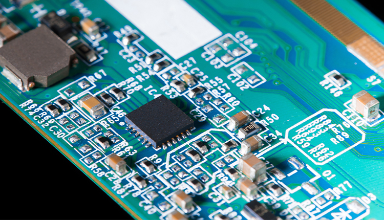
Printed Circuit Boards
Gold/Nickel/Copper/PCB; Tin/Copper/PCB; Gold/Nickel Phosphorus/Copper/PCB; Silver/Copper/PCB; Tin/Copper/PCB; Tin Palladium/Copper/PCB; Gold/Palladium/Nickel Phosphorus/Copper/PCB.

Connector Plating
In the electronics and electrical industry, protective and wear-resistant coatings for electrical contacts are on the rise. Serving as vital connector components, surface treatments enhance corrosion and wear resistance while optimizing transmission functionality. Copper alloy is the base material, with plating layers including tin, gold, silver, nickel, and palladium.
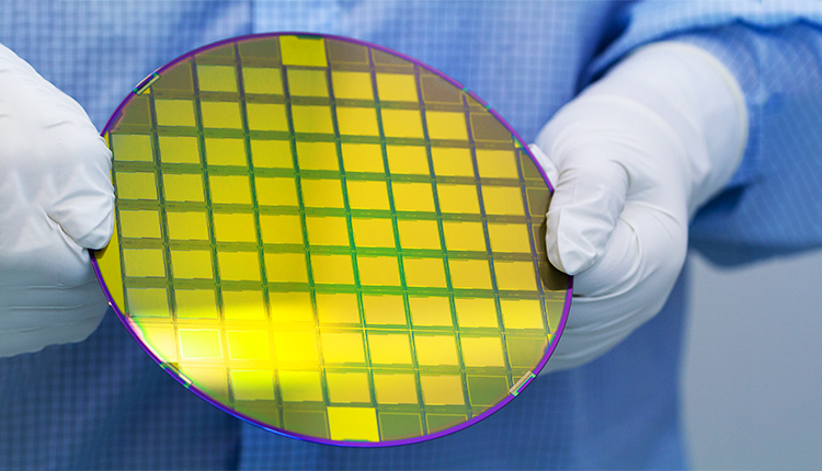
Wafer Manufacturing (Semiconductor)
A wafer, the base material for semiconductor chips, undergoes electroplating during fabrication. A conductive metal layer is deposited and processed into circuits. Uniformity and thickness of the coating are critical to meet strict specifications and ensure wafer quality.
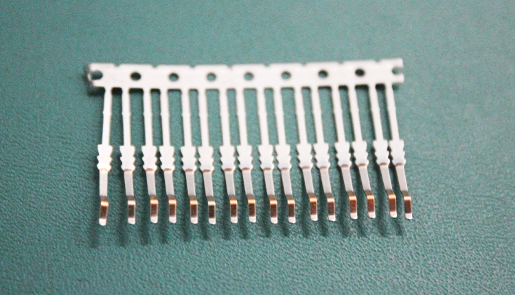
Lead Frame
The lead frame is a thin metal plate that connects internal chip contacts to external wires, serving as a primary structural material for semiconductor packaging. To ensure optimal bonding and mounting, special surface treatments are applied, with plating elements such as gold, silver, palladium, and nickel.
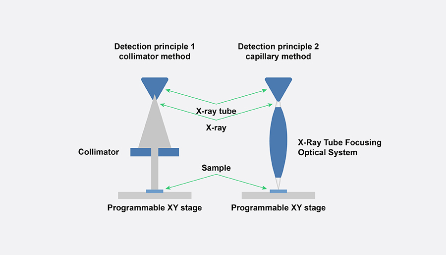
Multi-collimator
The system offers optional multiple collimators or automatically switches between collimator combinations via software. This flexibility allows seamless handling of parts with different sizes.
Up-bottom Design
The instrument features an up-bottom design, enabling quick, precise, stable, and efficient measurement of super-large, irregular, small, and even liquid samples with ease.
High Intensity X-ray Tube
INSIGHT can be outfitted with a high-intensity capillary optical system, enhancing the instrument's count rate, precision in point measurement, and capability to measure thinner coatings. This upgrade significantly boosts the analysis efficiency of the instrument.
Highly sensitive detector
For intricate coating structures, the SDD series detectors offer advantages in analyzing elements with XRF-like characteristics. These detectors provide better resolution, lower background noise (resulting in the highest signal-to-noise ratio), and enhanced accuracy in measuring thinner coatings.
Auto Focus
Samples are swiftly brought into focus within seconds, irrespective of their thickness or size. The instrument can measure samples from distances of up to 80 mm. It excels in measuring parts with recessed areas and is well-suited for measuring multiple samples at varying heights.
Programmable automatic displacement sample stage
The instrument features an automatic platform that facilitates seamless automatic measurements. This capability enables faster sample preparation and measurement, thereby boosting analysis throughput.
One-touch measurement
The instrument comes equipped with intuitive and intelligent analysis software, ensuring easy operation for users of all levels of expertise. Testing samples requires no specialized training; simply click "Start Test," and results are obtained within seconds.
Large measurement room
The slotted design (C-slot) of the instrument shell creates a spacious measurement area, facilitating easy placement of samples. This design accommodates large and flat items like printed circuit boards, as well as large samples with intricate shapes.
Increase productivity
INSIGHT automation accelerates sample measurements, boosting your throughput.
The characteristics of | Top-down measurement structure, XYZ measurement platform, MUTI-FP multilayer algorithm |
Scope of element | Na(11)—Fm(100) |
Analysis of the layer number of | 5 layers (4 layers + substrate) each layer can analyze 10 elements, composition analysis can analyze up to 25 elements |
X-ray tube | 50 W (50 kV, 1mA) micro-focused tungsten palladium ray tube (target material is optional) |
The detector | High sensitivity large area SDD detector, SDD 50mm2 large area detector, (optional) |
Collimator | Multiple collimators are optional, and multiple collimators can be combined |
The camera | High resolution CMOS color camera, 5 megapixels |
Manual sample XY platform | Moving range:100 x 150 mm |
Programmable XY platform | (Optional) |
Z-axis range of movement | 150 mm |
Sample bin size | 564×540×150mm(L x W x H) |
Overall dimensions | 664×761×757mm(L x W x H) |
Weight | 120KG |
The power supply | AC 220V±5V 50Hz (110V also available) |
Rated power | 150W |